 English
 Español
 中文
中文News
Home / News / Industry News / The Invisible Revolution: How Copper Tubes Became the Critical Battleground in Global Tech Supremacy
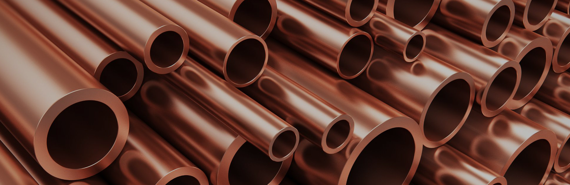
Subtitle: While the construction industry consumes 78% of global copper tube output, a handful of companies producing specialized tubes for AI chips and quantum computing achieve 50x price premiums—how did this 5% niche segment become strategically more important than the entire traditional market?
The global copper tube industry is experiencing unprecedented fragmentation. While traditional construction and HVAC applications grow at a modest 2-3% annually, demand for precision tubes in semiconductor manufacturing, AI infrastructure, and quantum computing is surging at 25-30% yearly. This divergence creates a two-tier market: bulk producers struggle with 3-5% margins, while specialized manufacturers command gross margins of 35-50% for tubes meeting extreme specifications.
The driving force is technological escalation. AI chips now generate heat densities exceeding 1,000 watts per square centimeter, requiring cooling solutions with precision unthinkable a decade ago. Quantum computing systems demand copper tubes with oxygen content below 5ppm and surface roughness under 0.8 micrometers—standards that push material science to its limits. Companies that master these specifications don't just supply components; they enable technological progress itself.

(This image was generated by AI.)
Table: The Copper Tube Market Split (2025)
|
Segment |
Traditional Construction |
High-Tech Applications |
Disparity Factor |
|
Growth Rate |
2-3% annually |
25-30% annually |
10x |
|
Price Point |
$7,000-9,000/ton |
$300,000-500,000/ton |
50x |
|
Key Spec |
Standard dimensions |
Oxygen ≤5ppm, Ra ≤0.8μm |
Beyond industry norms |
|
Margin Structure |
3-5% gross margin |
35-50% gross margin |
10-15x |
Conventional copper tube manufacturing hits physical limits when serving tech applications. Creating tubes for quantum computing requires controlling wall thickness to within ±0.003mm—a tolerance 10 times stricter than conventional precision engineering. These specifications aren't arbitrary; they determine whether qubits maintain coherence long enough for practical computation.
Leading manufacturers achieve this through hybrid approaches combining material science with advanced physics. Some use electron beam floating zone melting to achieve 99.999% purity, while others deploy laser interferometry to monitor production in real-time. The most advanced facilities operate in Class 1 cleanrooms where temperature fluctuates by less than 0.1°C annually—because even thermal expansion at the nanometer scale can ruin a tube's quantum suitability.
The innovation extends beyond purity to structural perfection. For semiconductor applications, tubes must maintain perfect internal surface continuity across kilometers of length, as any microscopic imperfection becomes a nucleation point for failure under extreme thermal cycling. This requires not just advanced manufacturing but entirely new quality assurance paradigms using AI-driven microscopy and atomic-level simulation.
Beyond commercial implications, advanced copper tubes have emerged as geopolitical assets. Nations leading in quantum computing, aerospace, and semiconductor manufacturing recognize that tube quality can determine technological sovereignty. This has triggered strategic investments and export controls reminiscent of the semiconductor industry a decade ago.
Countries with strong materials science capabilities now treat copper tube technology as critical infrastructure. Germany maintains dominance in medical-grade tubes through specialized engineering consortiums, while Japan's expertise in ultra-pure metals gives it an edge in semiconductor applications. The United States has classified certain copper tube manufacturing techniques as "emerging and foundational technologies" subject to export controls, particularly regarding quantum applications.
This geopolitical dimension reshapes supply chains. Companies can no longer simply purchase advanced tubes on open markets; they must navigate complex regulatory environments and form strategic partnerships. The result is a bifurcated market where geopolitical alignment increasingly determines technological access—a trend likely to accelerate as tubes become more sophisticated.
A profound tension exists between the extreme purity requirements of tech applications and sustainability goals. Producing oxygen-free copper (≤5ppm) typically requires energy-intensive processes like vacuum melting, with carbon footprints 3-5 times higher than conventional copper production. Meanwhile, the tech industry faces growing pressure to reduce emissions across its supply chain.
Innovators are responding with novel approaches. Some companies are developing electrochemical purification methods that achieve comparable purity with 60% less energy. Others are creating closed-loop recycling systems specifically for high-purity copper, recovering valuable material from manufacturing scrap without compromising quality. These solutions remain nascent but point toward reconciling technical requirements with environmental responsibility.
The challenge is particularly acute because tech applications often require virgin material rather than recycled content. Quantum systems are especially sensitive to isotopic variations that recycling can introduce. Solving this dilemma may require fundamentally new approaches to material design rather than incremental improvements to existing processes.
The most significant transformation may be the evolution of copper tubes from passive conduits to active system components. Researchers are developing tubes with embedded sensors that monitor temperature, pressure, and flow in real-time while maintaining perfect internal surfaces. These "smart tubes" don't just carry coolant; they become integral to thermal management systems, enabling predictive maintenance and dynamic optimization.
Further ahead lie more radical innovations. Some laboratories are experimenting with tubes whose internal surfaces are engineered at the atomic level to enhance heat transfer through quantum effects. Others are creating composite structures where copper layers alternate with materials like graphene to achieve thermal conductivity far beyond pure copper's limits. These approaches could make today's most advanced tubes seem primitive within a decade.
The ultimate frontier may be tubes that are manufactured and function in ways fundamentally different from current paradigms. 3D-printed tubes with optimized internal geometries impossible to create through traditional extrusion, or tubes that "heal" minor surface imperfections through embedded nanomaterials, could redefine what's possible in thermal management and beyond.
The copper tube's journey from commodity to critical enabler mirrors technology's broader evolution. As systems become more complex and demanding, components once considered mundane transform into sophisticated engineering challenges. The companies and nations that master these challenges will determine the pace of progress in fields from artificial intelligence to quantum computing.
This transformation also illustrates a broader principle: in advanced technology, there are no unimportant components. What appears to be a simple tube becomes a critical bottleneck when pushed to physical limits. Recognizing and solving these hidden challenges separates technological leaders from followers—and will continue to do so as we venture further into uncharted technological territory.

Copper Tube is made of high-purity copper material with a copper content of not less than 99.9%. The main material codes are T11050 and C12200(DHP), a...
See Details
Copper square tube is a metal tube with a hollow square cross-section. It is made of high-purity copper or copper alloy materials through multiple pre...
See Details
The Copper Water Tube produced by our company is a high-performance copper tube suitable for hot and cold water systems and heating applications. It h...
See Details
Copper capillary tube is usually manufactured by precision machining, and its dimensional accuracy can reach one thousandth of an inch. This ultra-hig...
See Details
The copper evaporator tube adopts a unique fin design, and the external fins are equipped with specially designed interconnected channels, so that eac...
See Details
Fin copper tube is a highly efficient heat exchange element. Its structural feature is that uniform fins are formed on the outer wall of the copper tu...
See Details![]() Tangpu Industrial Zone, Shangyu District, Shaoxing City, Zhejiang Province, China
Tangpu Industrial Zone, Shangyu District, Shaoxing City, Zhejiang Province, China
![]() +86-13567501345
+86-13567501345
© Zhejiang Jingliang Copper-Tube Products Co., Ltd All rights reserved.
